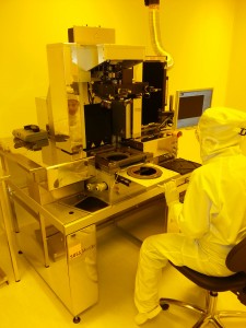
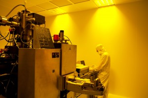
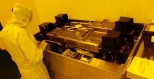
Definition of high precision patterns and structures on wafer, using lithography, is obtained with two main equipment:
ELECTRON BEAM VECTOR HB6 HR
Defines submicron and deep submicron process features definitions with the following reference parameters:
- This system is able to define submicron and deep submicron patterns and structures with the following reference parameters:
- Thermal Field Emission (TFE) electron gun
- High energy column (max 100kV)
- 25 MHz pattern generator
- 18 bits beam deflection
- Minimun beam spot size
- Maximum field size 0.524mm @100kV, 0.819mm @50kV Laser interferometer stage positioning correction
- Laser height measurement on substrate
- 32 levels dose assignment
- Temperature & mechanical vibration control
- Minimum linewidth: 30 nm ±20% (100μm field size @100keV)
- Stitching and overlay accuracy: ≤40 nm mean+3 sigma (500μm field size @100keV)
- 12-wafer air-lock capacity
- Piece-parts to 8’’ wafers, 6’’ mask capability
KARL SUSS MA6 BA6
This machine defines large patterns >0.7 µm and uses optical exposure system with tool set at 365 nm and has a guaranteed resolution of 0.7 µm. The system has the process capability to align front to back wafer surface with alignment accuracy ≤+/-1.5 µm


